Rapid PCB Prototyping with KiCad and a CNC Router
2025-07-22
Of all the PCB milling tutorials online, I didn't find one that goes into layout dos and don'ts when making a PCB on a CNC.
So, recently, I needed a quick PCB for a snooker scoreboard a friend of mine wanted hacked. The local club started streaming tournaments, and they needed a way to overlay their live scores.

I didn't want to return a hodgepodge of wires, floating resistors and modules. So I made the PCB, containing the additional electronics needed, on my router and while I was at it I wrote this guide. I didn't want to rediscover the whole process again in six months.
🔗Step by Step
Given how cheap boards are from China, spending hours on this is wasteful. I found out that the key to being fast is using a console tool like pcb2gcode. Here's an overview of the steps I came up with to mill a PCB quickly:
- At the PC
1.1 Schematic capture
1.2 Board layout
1.3 Export Gerbers & drill file
1.4 Runpcb2gcode - At the CNC
2.1 Set XY zero
2.2 Clamp PCB substrate in the vice
2.3 Chuck a V-bit, set Z zero
2.4 Mill traces
2.5 Chuck a drill bit, drill holes
- 1.3 and 1.4 can be combined in a single scripted step.
🔗KiCad: Schematic capture and PCB design
Circuit layout is no different than usual. But if you're making a PCB today you'll be using components you already have on hand. If you're going to be ordering parts, you might as well order a PCB too.
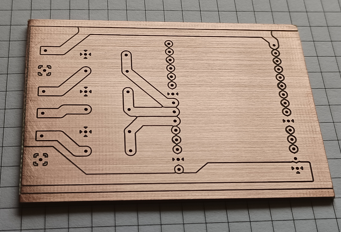
When you get to choosing footprints in the Schematic Editor, stick to through-hole parts with similar drill sizes. Matching hole sizes mean you can drill everything with a single bit, saving tons of time at the CNC. It may also be impossible to find all footprints with the exact same drill size, unless you make your own. 0.8mm drill works for small signal stuff like 1/4 watt resistors, TO-92 transistors and all pinheaders and DIP packages. If you have larger devices like a TO-220 voltage regulator, go for 1mm drill for everything.
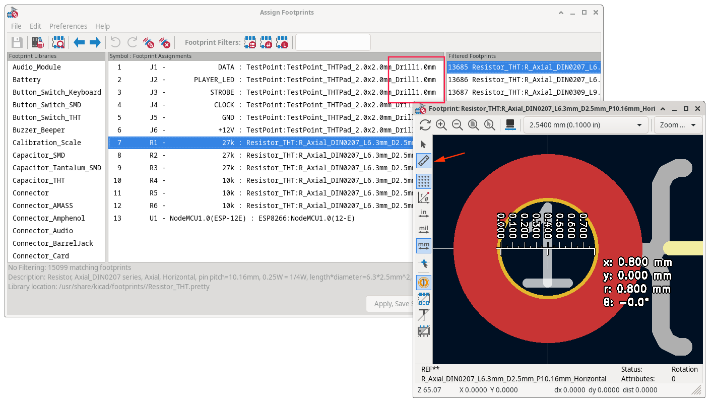
Notice how some part names contain the drill size. If they don't you can right click → View Selected Footprint and use the measure tool.
In the PCB Editor, start by drawing the outline of the PCB stock in the Edge.Cuts layer. The outline top-left corner must start at (0,0):
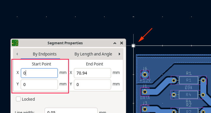
This produces more consistent results than letting pcb2gcode determine where 0,0 is. Next, import all components on the top layer.
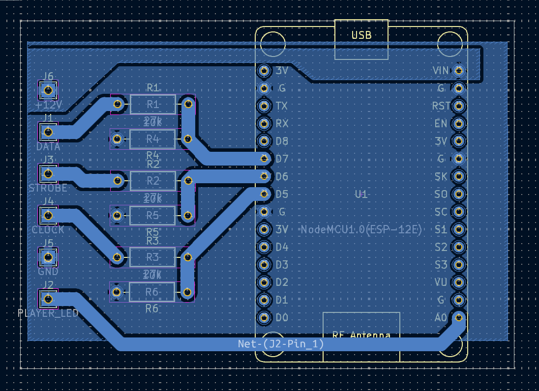
Group related circuit elements together and fiddle with positioning until no nets cross each other. This is important since we're only routing on the bottom layer. If that's not possible, try to minimize rats nest crossings. The top side of the PCB can be used for jumper wires.
When routing for milling, use the widest traces possible. 1mm, 2mm and wider, the machine doesn't care, but later you won't be soldering leads to small fragile strips of copper. You can use copper pours for routing too. Since the tolerances on desktop CNC routers aren't great, the V-bit might dig deeper in some parts, leaving thinner traces. Spindle runout can also cause the bit to cut more than intended. All of that adds up, wide traces are much more forgiving.
Set up the entire back side as one big GND pour. Then, increase the thermal spoke width to be larger than 1mm. This avoids small features and gives more room for error if a larger drill is used for the holes.
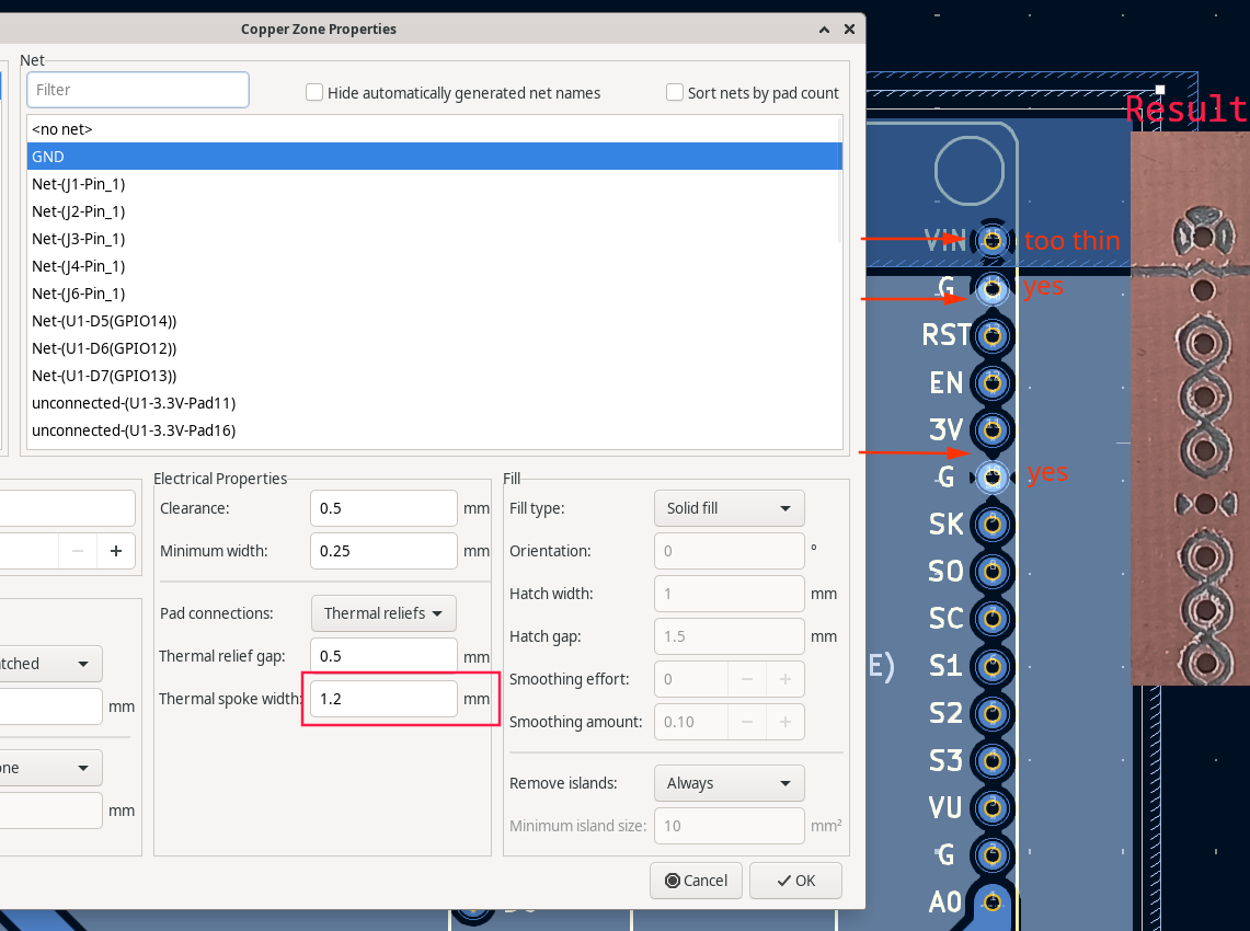
Notice in the above image how thin spokes combined with bad tolerances produced almost an unworkable pad.
Tight tolerances and fine traces are achievable, but that takes time and money. And laying a huge trace while designing is free. You can do double sided boards too, but it takes longer and is more finicky. If a design needs two layers, it's almost always better to send it to a fab.
🔗Exporting gcode files
First, generate gerber files. These are the same used to order from a vendor. There are no specific settings, just:
KiCad PCB Editor → File → Fabrication Outputs → Gerbers
- Set "Output directory" to "gerbers/"
- Select only B.Cu (bottom copper)
- Click Plot
- Then Generate Drill Files → Generate
Everything up to this point has to be done when ordering from a prototyping service too.
Next, create a millproject file in the project directory. You only need to get this right once and can later just copy that file in another project. pcb2gcode searches for that file and is a convenient way to provide all the arguments while keeping them close to the KiCad files.
Example millproject file:
back=gerbers/<Project Name>-B_Cu.gbr
drill=gerbers/<Project Name>.drl
# outline=gerbers/addon_board-Edge_Cuts.gbr

# Generic
metric=true         # use metric units for parameters
metricoutput=true   # use metric units for output
nog64=true          # do not set an explicit g64
nom6=true           # do not emit m6
zsafe=2             # The height in mm at which the bit can move freely without obstruction
zchange=35          # Tool changing height in mm
output-dir=gcode

# Place a 5x7cm board in the lower right quadrant of the coordinate system
# This will allow you to probe the fixed jaw of the vise for (0,0) on the CNC.

mirror-axis=35.5    # set this to half of your board width

# Drilling
zdrill=-2.5         # drilling depth
drill-feed=200      # Vertical mm/min feed
drill-speed=24000   # Spindle RPM
onedrill=true       # Use a single drill for all holes
nog81=true          # replace G81 with G0+G1 (no G81 in GRBL)

# Milling
zwork=-0.1          # V-bit plunge depth
#mill-diameters=0.11 # 60 deg V-bit dia at -0.1 plunge depth
#mill-diameters=0.08 # 45 deg V-bit dia at -0.1 plunge depth
mill-diameters=0.05 # 30 deg V-bit dia at -0.1 plunge depth
mill-speed=24000    # Spindle RPM
mill-feed=600       # Horizontal feedrate in mm/min
mill-vertfeed=100   # Plunge rate in mm/min
voronoi=true        # cuts the milling time significantly, but check with this on and off if everything looks ok
preserve-thermal-reliefs = true # has effect only if voronoi=true

# Cutting
# zcut=-2.5
# cutter-diameter=2
# cut-feed=80
# cut-infeed=100
# cut-speed=24000
# cut-side=back
Then, in your project directory create a gcode folder and run:
docker run --rm -i -t -v ".:/data" ptodorov/pcb2gcode
Package managers may have older versions of
pcb2gcode. And I had trouble installing it. This docker image contains the correct versions ofpcb2gcodedependencies.
Load the output into ncviewer.com (or your G-code viewer of choice) and inspect:
gcode/back.ngcgcode/drill.ngc
Make sure nothing looks off. See if any toolpaths risk hitting clamps or limits. Look at the grid to check for unit and scaling errors. The generated gcode should match your PCB design and its size.
This feedback cycle is quick: change something in KiCad, run pcb2gcode, drag files in viewer. You can get a good feeling of what does what and what will happen on the machine. Try turning voronoi off and on, explore the wiki as well.
Going a step further, a small bash script can automate exporting gerbers and running pcb2gcode:
#!/bin/bash

set -e

filename=$(basename -- "$1")
filename="${filename%.*}"

kicad-cli pcb export gerbers -o output -l B.Cu $1
kicad-cli pcb export drill -o output $1

mkdir -p gcode

docker run --rm -i -t -v ".:/data" ptodorov/pcb2gcode --back="output/$filename-B_Cu.gbl" --drill="output/$filename.drl"
Then run it by providing the .kicad_pcb file as a first argument:
$ chmod +x export.sh
$ ./export.sh <KiCad Project Name>.kicad_pcb
🔗At the CNC
Depending on your minimum trace width, clearances, and part lead pitch, you might not need to probe a bed mesh. That should be the case if you have your vice leveled and spindle trammed. If no traces go to the edge of the board you can skip the wasteboard too and just clamp it in the vice.

Set your CNC's (0,0) to the upper left corner of the fixed jaw or to the edge of the copper clad board if using a wasteboard. When using a vice clamp it gently. If it's too tight the fiberglass will bend enough to ruin traces.
Steps:
- Clamp the substrate in the vise
- Insert and tighten a V-bit
- Probe and set Z zero
- Run the
back.ngcfile - After milling is finished, change the v-bit for a drill bit
- Probe and set Z zero again on the drill bit
- Run the
drill.ngcfile
🔗Finally, this feels like breadboarding
After a few boards, it takes 20 to 30 minutes from viewing at a design in KiCad to holding it in your hand.
I think of this as a more permanent version of breadboarding than a replacement for professionally made boards. On a breadboard you start with a lot of constraints like number of components, types of components, parasitic capacitance and circuit complexity. And you work around them to test a circuit. It is the same with milled PCBs, but with a different set of tradeoffs.